


Reflow Soldering Guidance for Surface-Mount Components
The optimal reflow profile for soldering ICE SMT components depends on more than just the selected component and solder paste. In fact, a wide range of factors, such as component size, thermal mass, board layout, and pad design, all significantly influence thermal behavior during reflow. For instance, these factors often have competing requirements: larger components may require higher peak temperatures or longer soak times to ensure proper wetting, while smaller packages may simultaneously need slower ramp rates or controlled cooling to avoid thermal damage.
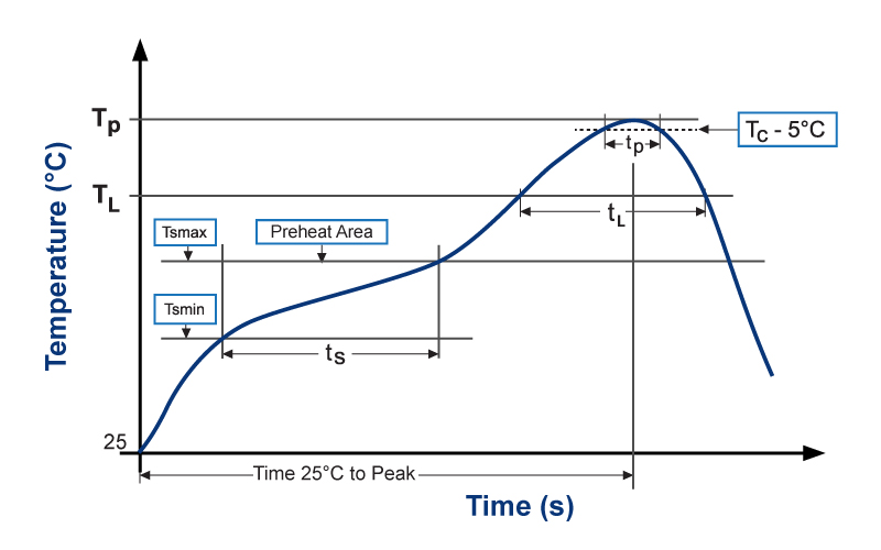
To help navigate these variables, Table 1 provides general starting points for profile development. However, these are only guidelines and must be refined based on the customer’s chosen solder alloy, component density, and the specific thermal characteristics of the assembly. Ultimately, because this complex interplay of factors means no single profile suits all board designs, ICE Components recommends validating and optimizing the reflow process for each application. This validation is critical to ensure both solder joint integrity and long-term reliability.
| Table 1: Reflow Soldering Profile (Lead-Free) | |
|---|---|
| Preheat/Soak Temperature, Min (TSMIN) | 150°C |
| Preheat/Soak Temperature, Max (TSMAX) | 200°C |
| Time (tS) from TSMIN to TSMAX | 60 – 120 sec |
| Ramp-Up Rate (TL to TP) | 3°C/sec max |
| Liquidous Temperature (TL) | 217°C |
| Time (tL) maintained above TL | 60 – 150 sec |
| Peak Package Body Temp (TP) | TP ≤ TC |
| Time (tP) within 5°C of the specified classification temperature (TC) |
< 30 sec |
| Ramp-Down Rate (TP to TL) | 6°C/sec max |
| Time 25°C to peak temperature | 8 min max |
| Table 2: Lead-Free – Classification Temperature (Tc) | |||
|---|---|---|---|
| Package Thickness | Volume mm3 (<350) | Volume mm3 (350 – 2000) | Volume mm3 (>2000) |
| <1.6 mm | 260°C | 260°C | 260°C |
| 1.6 mm – 2.5 mm | 260°C | 250°C | 245°C |
| > 2.5 mm | 250°C | 245°C | 245°C |
Wave Soldering Guidance for Through-Hole Components
Important: ICE THT components are specifically designed for wave soldering and are not compatible with reflow processes. Reflow soldering typically subjects components to higher peak temperatures and extended dwell times, which may exceed their thermal limits and compromise long-term reliability.
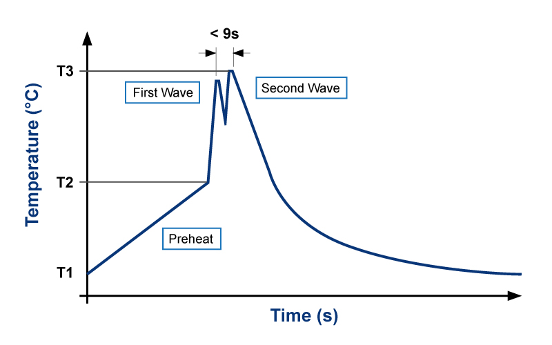
While ICE Components does not mandate a fixed wave soldering profile, we provide baseline parameters to support thermal profiling and process development. The operator must adjust the soldering profile for each application, considering solder type, flux, board design, component size, and heat tolerance. The most temperature-sensitive part on the PCB sets the limits for peak temperature and exposure time.
Note: These values are intended as starting points. Process engineers adjust parameters by considering equipment capability, board complexity, and component layout. Validation under actual production conditions is critical to ensure solder joint reliability and long-term mechanical and electrical performance.
| Table 3: Wave Soldering Profile (Lead-Free) | |
|---|---|
| Max. Preheat Ramp Rate | 1 – 4°C/sec |
| Max. Preheat Temperature (T2) | 80 – 140°C |
| Bottom Side Contact Time | < 9 sec |
| Cooling Rate | < 6°C/sec |
| Time from T1 to T2 | 60 – 180 sec |
| Ambient Temperature (T1) | 25 – 40°C |
| Peak Wave Temperature (T3) | 270 ± 5°C |
RoHS Compliance
The reflow and wave soldering profiles provided are designed to support RoHS-compliant, lead-free assembly processes. These profiles reflect industry-standard thermal parameters suitable for common lead-free alloys. However, due to variations in alloy composition, board design, and process equipment, users must validate profile compatibility against their specific materials and production environment. This ensures optimal solder joint integrity and long-term reliability.
Have questions about soldering ICE Components? You can reach out to our team for personalized support.