
- Home
- Inductors
- High-Current Flat-Wire Power Inductors
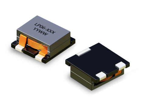
- LP06 SERIES: SMT High-Current Flat-Wire Power Inductors
Key Features
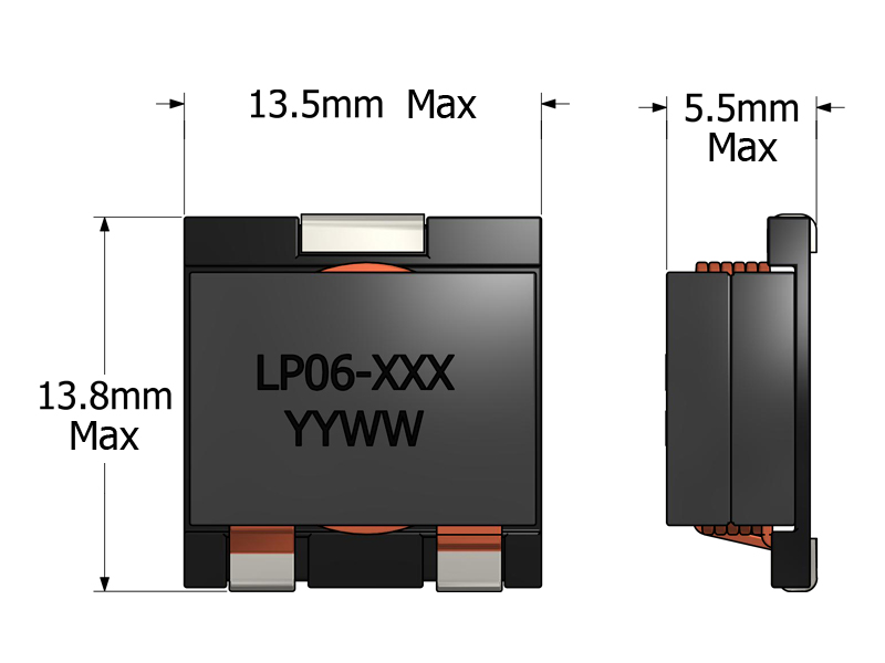
- Footprint 13.5 × 13.8 mm with 5.5 mm height for compact layouts
- Saturation rating up to 75 A for high-current power rails
- Inductance options from 100 nH to 7200 nH for flexible filtering
- Supports switching frequencies up to 1 MHz for modern converter stages
- Low-DCR winding improving efficiency under load
- Magnetically shielded construction reducing EMI
- SMT package supporting automated pick-and-place assembly
APPLICATIONS
- VRMs and POL converters in server and embedded systems
- High-current DC/DC stages for core and auxiliary power rails
- Low-EMI power modules using magnetically shielded inductors
- Rail filtering and output choke in compact power supplies
- Dense PCB layouts needing efficient SMT inductors
- Industrial and telecom equipment requiring stable high-current magnetics
Electrical Specifications @ 25°C - Operating Temperature Range1: -40°C to +130°C
Part Number
Inductance2
(nH, ±10%)
DCR (mΩ, Typ.)
ISAT3(A)
IDC4 (A)
Mechanical Drawing
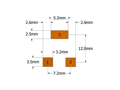
Recommended PCB Layout
Schematic

-
Operating Temp. Range: The combination of ambient temperature and temperature rise.
-
Inductance: Tested at 1MHz, 0.1 VRMS.
-
ISAT: DC current through the winding to cause a 10% (typ) drop in inductance.
-
IDC: DC current through the winding to cause a 40°C (typ) temperature rise at 25°C ambient. PCB layout, trace thickness and width, airflow and proximity to other devices will affect the temperature rise.
-
Flammability Standard: Meets UL 94V-0.
-
PACKAGING
- Reel Diameter: 13″
- Reel Width: 24mm
- Pieces/Reel: 600
-
Specifications subject to change without prior notice.
Frequently Asked Questions (FAQs)
What physical design element of LP06 supports its high current rating?
The LP06 uses a low-austenitic copper winding with a relatively large cross-section and optimally gapped ferrite core. This combination reduces DC resistance and core losses, enabling high continuous current without undue heating or loss — provided the PCB layout supports sufficient copper for heat dissipation.
How does DC bias affect inductance and ripple current in the LP06?
As DC load current increases toward the part’s saturation threshold, the effective inductance decreases. This inductance roll-off increases ripple current, which can stress downstream components (e.g., output capacitors) if not accounted for in the design. Operating with margin below saturation helps keep ripple predictable.
What layout considerations improve thermal behavior when using LP06?
Ensuring adequate copper area around the inductor pads, incorporating thermal vias under or around the inductor, and maintaining airflow over the component all help reduce hotspot temperature. Poor thermal design can undercut the rated IDC performance even if electrical ratings are met.
Why is trace symmetry important when LP06 is used in parallel or multi-phase converters?
In parallel or multi-phase configurations, differences in trace length, copper width, or via count can produce uneven current sharing. For balanced load distribution and minimized thermal stress, symmetrical routing between parallel inductors or phases is critical.
How should designers account for core losses at high switching frequencies?
Even though LP06 supports high switching frequencies, ferrite core losses increase with frequency. Designers should check core and copper loss performance at intended operating frequency and include these loss components in efficiency and thermal models.
What are the trade-offs of using LP06 versus a larger inductance part?
LP06 targets low impedance and high current. In return, it provides lower energy storage than higher-inductance parts. For applications where energy storage and low ripple at low switching frequency are prioritized over current capacity, alternative higher-inductance series may be preferable.
How does temperature affect LP06 inductance and resistance over time?
As temperature rises, copper resistance increases and core permeability shifts, which can slightly affect inductance and increase conduction loss. Careful PCB thermal design and device placement help mitigate temperature-driven performance shifts.
What factors should engineers verify in simulation models involving LP06?
Include real DCR, inductance derating under DC bias, frequency-dependent core loss, and thermal resistance. Idealized inductors in simulations can underestimate ripple and overestimate efficiency.
Will LP06 performance degrade under repeated transient surges?
Short surge currents may be absorbed if the part remains within thermal and saturation limits. However, frequent surges at or near saturation current can cause heating, core stress, and gradual loss of inductive performance. A margin between design peak current and ISAT is advised.
How can LP06 be affected by proximity to high-dv/dt nodes on the PCB?
High-dv/dt switching edges near the inductor can induce noise into adjacent traces or contribute to EMI if layout is not managed. Maintaining proper clearance and using ground shielding or copper pours for return paths help minimize coupling and improve overall signal integrity.