
- Home
- Inductors
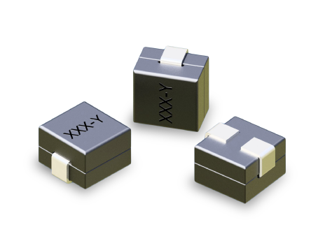
- High-Current Ferrite-Bead Power Inductors
- LP02-1 SERIES: SMT High-Current Ferrite-Bead Inductors
Key Features
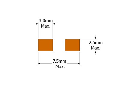
- Ultra-compact 7.0 × 6.5 mm max footprint and 5.0 mm low profile
- One-turn SMT inductor optimized for high-current VRMs and POLs
- Saturation current up to 40 A for demanding DC/DC converter workloads
- Low DCR enabling high efficiency and low thermal loss under load
- Designed for up to 1 MHz high-speed switching frequency
- SMT construction supporting automated pick-and-place assembly
- Design verified by leading IC manufacturers
APPLICATIONS
- Voltage Regulator Modules (VRMs) for CPUs, GPUs, and SoCs
- Synchronous buck/boost DC/DC converters for servers and embedded systems
- Point-of-Load (POL) converters supplying high current to downstream rails
- High‑frequency, high‑current power supplies for telecom and industrial use
- Compact power modules requiring minimal footprint and automated assembly
Electrical Specifications @ 25°C - Operating Temperature Range1: -40°C to +130°C
Mechanical Drawing

Recommended PCB Layout
Schematic

-
Operating Temp. Range: The combination of ambient temperature and temperature rise.
-
Inductance: Tested at 1MHz, 0.1 VRMS.
-
Tighter DCR tolerances available. Contact ICE for more details.
-
ISAT: DC current through the winding to cause a 15% (typ) drop in inductance.
-
IDC: DC current through the winding to cause a 40°C (typ) temperature rise at 25°C ambient. PCB layout, trace thickness and width, airflow and proximity to other devices will affect the temperature rise.
-
PACKAGING
-
Reel Diameter: 13″
-
Reel Width: 16mm
-
Pieces/Reel: 1000
-
-
Specifications subject to change without prior notice.
Frequently Asked Questions (FAQs)
What current handling does LP02-1 support?
LP02-1 inductors support saturation currents up to 40 A (some variants tested up to 85 A per datasheet) while maintaining low DCR, making them suitable for high-current POL or VRM rails.
What switching frequencies can LP02-1 handle reliably?
The LP02-1 is designed for switching frequencies up to about 1 MHz, which makes it suitable for modern high-frequency DC/DC converters and buck regulators.
How compact is the LP02-1 package and why does that matter?
It has a maximum footprint of 7.0 × 6.5 mm (or 7.2 × 6.5 mm depending on variant) and a low profile of 5.0–5.2 mm — this compact form allows dense PCB layouts and aids automated SMT pick-and-place assembly.
What makes LP02-1 suitable for high-current, space-constrained designs?
Because of its single-turn, high-current SMT inductor design, low DC resistance, and small footprint, LP02-1 delivers high current capacity with minimal thermal loss and space overhead — ideal for POL converters, VRMs, and compact DC/DC modules.
What are the DC and thermal limits under continuous load?
The datasheet defines a “IDC” rating (current for 40 °C temperature rise from 25 °C ambient) — for many LP02-1 variants this is around 42 A, but real performance depends on PCB layout, copper trace width, airflow, and thermal management on the board.
Are there trade-offs when using a one-turn SMT inductor like LP02-1 versus a multi-turn or larger inductor?
Yes — while LP02-1 excels in current handling and compact size, its low inductance (in the nH range) means it’s optimized for high-current, low-inductance applications (e.g. POL converters), not for high-inductance filtering or energy storage. Designers must verify that inductance value and current rating match their ripple and load requirements.
How does PCB layout affect LP02-1 inductor performance?
Because of the high currents involved, trace width, via count, and copper area around the inductor must be adequately sized. Poor layout can lead to excessive heating, voltage drop, or thermal stress despite the inductor’s own ratings.
Can LP02-1 support both DC output filtering and high-frequency switching environments?
Yes — LP02-1’s design supports stable performance under DC bias and also performs at high switching frequencies up to 1 MHz, making it flexible for a variety of converter topologies including synchronous buck regulators and high-frequency POL modules.
What system-level design considerations should engineers verify when selecting LP02-1?
Engineers should check peak and continuous load current, required output ripple/inductance, PCB copper and thermal layout, and switching frequency to ensure the inductor meets current handling and efficiency targets without thermal or magnetic stress.
When is LP02-1 preferred over larger inductors or different series?
LP02-1 is ideal when size, automated SMT assembly, high current capacity, and low thermal loss are more important than high-inductance energy storage — e.g. in point-of-load converters, VRMs for CPUs/GPUs/SoCs, telecom power rails, or compact power modules.